• Skip navigation
  • Skip to navigation
  • Skip to the bottom
Simulate organization breadcrumb open Simulate organization breadcrumb close
Institute I: General Materials Properties
  • FAUTo the central FAU website
  1. Friedrich-Alexander-Universität
  2. Faculty of Engineering
  3. Department Materials Science and Engineering
  • en
  • de
  • Campo
  • UnivIS
  • Jobs
  • Map
  • Help
  1. Friedrich-Alexander-Universität
  2. Faculty of Engineering
  3. Department Materials Science and Engineering

Institute I: General Materials Properties

Navigation Navigation close
  • Institute
    • Team
    • Contact & Directions
    • History
    • Job Offers
    Portal Institute
  • Research
    • Atom Probe Tomography & 3D-Nanoanalytics
    • High Temperature Materials
    • Light Metals & Mechanical Testing
    • Modelling & Simulation
    • Nanomechanics
    • Nanostructured Materials
    • Publications
    • Current cooperations
    Portal Research
  • Education
    • Lectures and seminars
    • Retreat Symposium – Sattelbogen
    Portal Education
  • Equipment
    • Heat treatments
    • Metallography and sample preparation
    • Microscopy and analysis
    • Mechanical testing
    • Tribological properties
    • Generation of nanostructured materials
    • Simulation
    • Other equipment
    Portal Equipment
  • Downloads
    • Tools
    • Newsletter
    Portal Downloads
  1. Home
  2. Equipment
  3. Microscopy and analysis
  4. Transmission electron microscope – Philips CM200

Transmission electron microscope – Philips CM200

In page navigation: Equipment
  • Heat treatments
  • Metallography and sample preparation
  • Microscopy and analysis
    • Atom probe – Cameca Leap 4000X HR
    • Atom probe – Oxcart
    • Atomic force microscope – Bruker Dimension 3100
    • Dynamic differential calorimetry for thermal analysis (DSC, Netsch 204 F1 Phoenix®)
    • Field ion microscope (FIM)
    • Large chamber scanning electron microscope (LC-SEM)
    • Scanning electron microscope with FIB – Zeiss Crossbeam 1540
    • Scanning electron microscope with FIB- FEI Helios NanoLab 600i DualBeam
    • Transmission electron microscope – Philips CM200
    • X-Ray diffractometer – Bruker D5000
  • Mechanical testing
    • high-frequency pulsator – Zwick Roell
    • Hysitron Triboscope
    • In-situ Nanoindenter – Femtotools FT-NMT03
    • Mechanical testing of thin films – Bulge Test
    • Nanoindenter – Agilent XP
    • Nanoindenter – KLA-Tencor G200
    • Nanoindenter- FT-NMT04 IN-SITU SEM
    • Netzsch TMA Hyperion 402 F3 Hyperion
    • Pneumatic mechanic creep machines
    • Servohydraulic fatigue test systems – MTS810/880
    • Ultrasonic fatigue system Ultrafast-WKK
    • Universal Testing Machines – Instron
  • Tribological properties
  • Generation of nanostructured materials
    • Accumulative Roll Bonding
  • Simulation
  • Other equipment
    • CNC milling machine – Pocket NC
    • Filament 3D printer
    • PVD evaporation unit EVU-MSE-1
    • stereolithography3D printer- Formlabs Form 3

Transmission electron microscope – Philips CM200

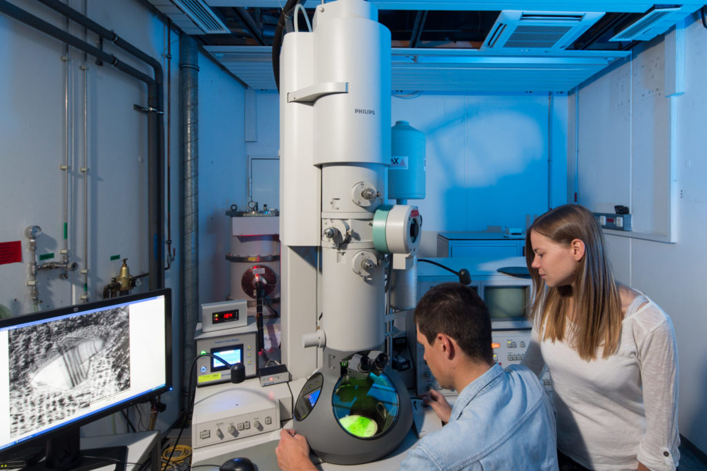
The Philips CM200 can be used in TEM and STEM mode at high voltages up to 200 kV. In the TEM mode, images are taken with a 2k x 2k CMOS camera from TVIPS with quick readout times of up to 1.8 fps. For crystallographic investigations, two double-tilt holders are available, which are able to cover a large angular range (α ± 40°,β ± 30°). Additionally, the chemical composition can be determined in the STEM mode through EDS in either quantitative point measurements or qualitative area scans.

  • LaB6 cathode
  • High tension – 200 kV
  • 2k x 2k CMOS camera F216 (TVIPS)
  • EDS detector (EDAX)


Verantwortlicher Mitarbeiter:

Andreas Bezold

Department of Materials Science and Engineering
Chair of General Materials Properties

  • Phone number: +49 9131 85-27485
  • Email: andreas.bezold@fau.de
Friedrich-Alexander-Universität
Erlangen-Nürnberg

Martensstraße 5
91058 Erlangen
  • Legal notice
  • Privacy
  • Accessibility
Up