• Skip navigation
  • Skip to navigation
  • Skip to the bottom
Simulate organization breadcrumb open Simulate organization breadcrumb close
Friedrich-Alexander-Universität Institute for General Materials Properties MSEI
  • FAUTo the central FAU website
  1. Friedrich-Alexander-Universität
  2. Technische Fakultät
  3. Department Werkstoffwissenschaften
Suche öffnen
  • en
  • de
  • Campo
  • StudOn
  • FAUdir
  • Jobs
  • Map
  • Help
  1. Friedrich-Alexander-Universität
  2. Technische Fakultät
  3. Department Werkstoffwissenschaften
Friedrich-Alexander-Universität Institute for General Materials Properties MSEI
Navigation Navigation close
  • Institute
    • Team
    • Contact & Directions
    • History
    • Job Offers
    Portal Institute
  • Research
    • Atom Probe Tomography & 3D-Nanoanalytics
    • High Temperature Materials
    • Light Metals & Mechanical Testing
    • Materials for Hydrogen and Energy Applications
    • Nanomechanics
    • Nanostructured Materials
    • Publications
    • Current cooperations
    Portal Research
  • Education
    • Lectures and seminars
    • Retreat Symposium – Sattelbogen
    Portal Education
  • Equipment
    • Heat treatments
    • Metallography and sample preparation
    • Microscopy and analysis
    • Mechanical testing
    • Tribological properties
    • Generation of nanostructured materials
    • Simulation
    • Other equipment
    Portal Equipment
  • Downloads
    • Tools
    • Newsletter
    Portal Downloads
  1. Home
  2. Equipment
  3. Microscopy and analysis
  4. Scanning electron microscope with FIB- FEI Helios NanoLab 600i DualBeam

Scanning electron microscope with FIB- FEI Helios NanoLab 600i DualBeam

In page navigation: Equipment
  • Heat treatments
  • Metallography and sample preparation
  • Microscopy and analysis
    • Atom probe - Cameca Leap 4000X HR
    • Atom probe - Oxcart
    • Atomic force microscope - Bruker Dimension 3100
    • Dynamic differential calorimetry for thermal analysis (DSC, Netsch 204 F1 Phoenix®)
    • Field ion microscope (FIM)
    • Large chamber scanning electron microscope (LC-SEM)
    • Scanning electron microscope with FIB - Zeiss Crossbeam 1540
    • Scanning electron microscope with FIB- FEI Helios NanoLab 600i DualBeam
    • Transmission electron microscope - Philips CM200
    • X-Ray diffractometer - Bruker D5000
  • Mechanical testing
  • Tribological properties
  • Generation of nanostructured materials
  • Hydrogen analytics
  • Simulation
  • Other equipment

Scanning electron microscope with FIB- FEI Helios NanoLab 600i DualBeam

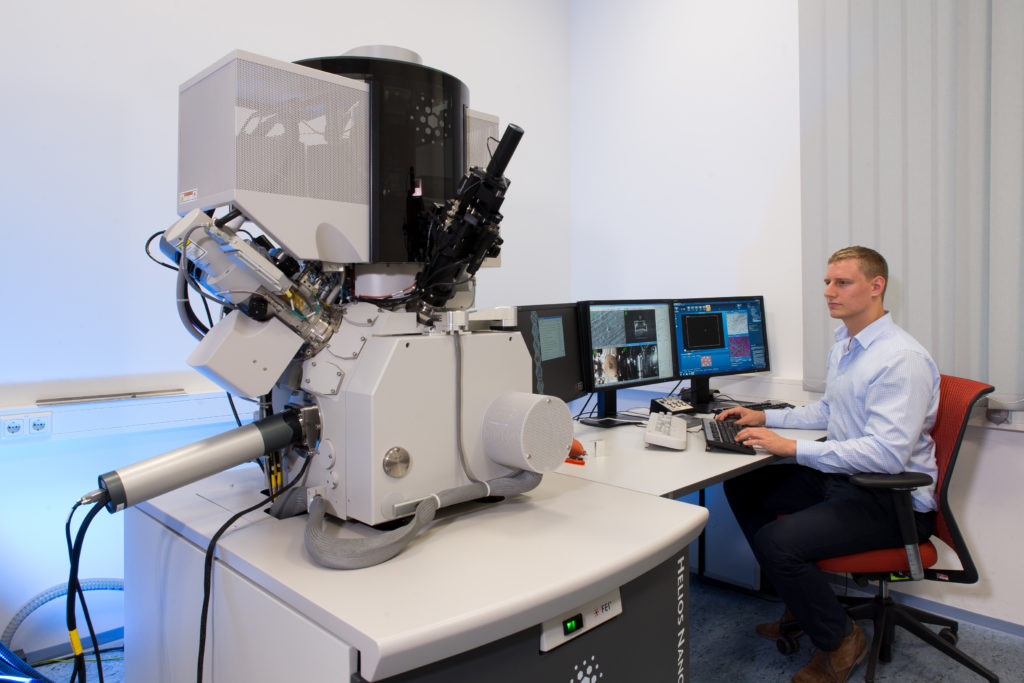
Helios NanoLab 600i FIB Workstation with SE-,BSE-,STEM-, EBSD- und EDS-detector: many institutes from FAU are working together on this high-resolution Scanning Electron Microscope with field emission and FIB technology to achieve findings on new concept for lightweight materials and manufacturing processes, i.e. additive manufacturing. The aim is to work interdisciplinary on innovative concepts for engineering materials to obtain better knowledge about the relation of microstructure and bulk properties. For this purpose 3D-analysis of microstructures, innovative in-situ experiments and preparation of electron-transparent samples are realized.


Responsible employees:

Julian Völkl, M. Sc.

Department of Materials Science and Engineering
Chair of General Materials Properties

  • Phone number: +49 9131 85-27486
  • Email: julian.voelkl@fau.de

Simon Helmert, M. Sc.

Department of Materials Science and Engineering
Chair of General Materials Properties

  • Phone number: +49 9131 85-25240
  • Email: simon.helmert@fau.de

Addition information

50 years Institute I: GMP

Materials science in Erlangen

https://www.youtube.com/watch?v=rbT0kc5qacM
Friedrich-Alexander-Universität
Erlangen-Nürnberg

Martensstraße 5
91058 Erlangen
  • Legal notice
  • Privacy
  • Accessibility
  • Facebook
  • RSS Feed
  • Twitter
  • Xing
Up